HTP!m Devlog 3: Soldering, PCBs, Firmware, Foundation, K8s, and Web Dev
I’m gonna be keeping this devlog short since I have a lot of work to do. Since the last devlog, we’ve made more progress on the project in a few tracks: we’ve made some great leaps in design and assembly of the electronics related to the set; we’re still working on the firmware and related scripts for the embedded systems; we laid out the foundation of the set; we got a Kubernetes cluster up; and we made more progress on the web platform.
Soldering
After last week’s blog post, Noor and I knocked out the assembly of the last 2 HTP!m MODCORE circuits. Ivan, Noor, and another one of our friends at HackMerced, Alisson, are going to be coming over during the next sprint to solder and assemble some more circuits I have designed. Speaking of which…
PCBs
I finished the design of 3 more PCBs for the project, each related to the HTP!m CONTROL unit.
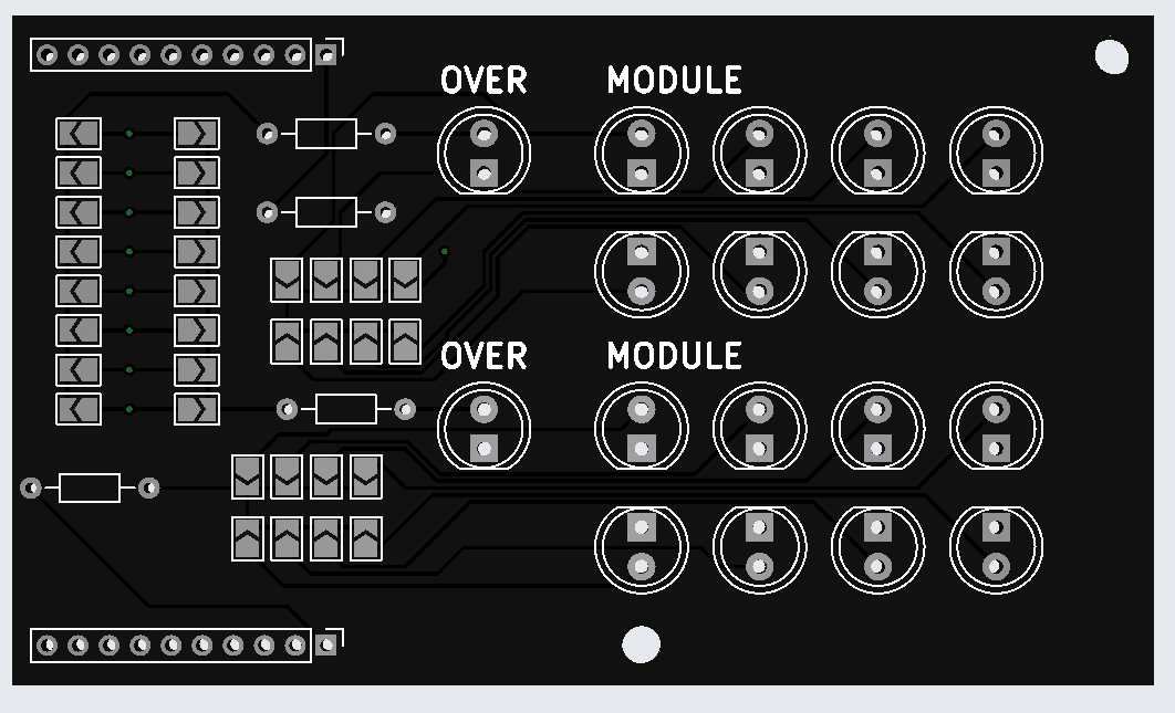
HTP!m CONTROL Module Display
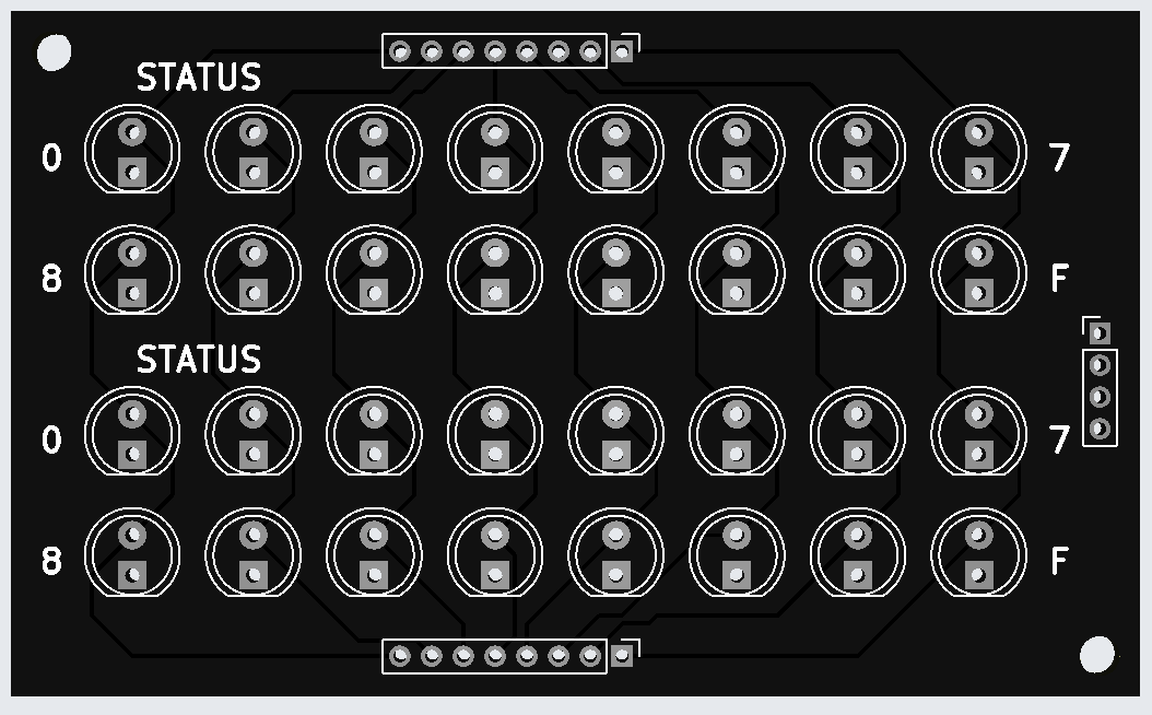
HTP!m CONTROL Module Status
HTP!m CONTROL Numericals
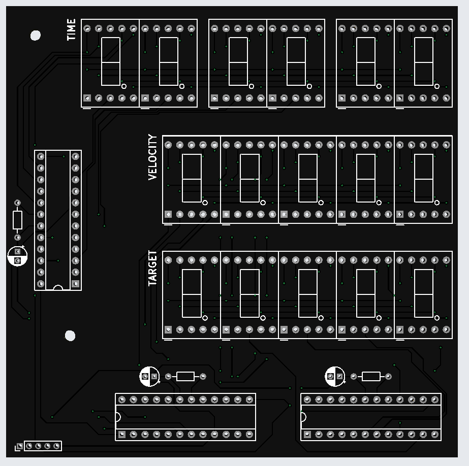
Based on my measurements, these should be able to just barely fit very snugly into the HTP!m CONTROL display panel. I’ll need to create a 3D CAD of screw sockets for the PCBs to be mounted to so that I can 3D print it. This is not one-to-one with the original design in Figma because I needed to prioritize functionality during the design of the PCBs. In addition, in order to save time, I made these PCBs black and we’re doing to scrap the idea of a cover panel on top of them. Besides, the exposed-PCB aesthetic would probably look cool.
The reason why I opted to make multiple PCBs instead of one large PCB is because I use JLC PCB (not sponsored) to make my PCBs, and their prices are super cheap for any PCB smaller than 100 mm x 100 mm. Besides, their minimum order quantity is 5 PCBs. It just made more sense for me to break up the display panel into multiple, smaller PCBs, with some parts replicable.
The Module Display just uses good ol’ SN74HC595N shift registers and solder bridges. I’m using MAX7219 ICs to handle multiplexing of a large number of LEDs for the other 2 PCBs. Related groups are daisy-chained together. For example, all the numericals are daisy-chained with each other, and all the module statuses are daisy-chained with each other. In order to prevent needing to push too many bits all at once, I made the decision to keep the module statuses on a separate CS line than the numericals.
I put the order in for these PCBs last Monday night and they’re arriving next Monday by end-of-day. We have a solder sesh planned to knock out the assembly of these. I have the parts ready for us already. Here’s to hoping all goes smoothly!
I still have 2 more PCBs to prototype, design, and order. Hopefully I’ll get it done by the end of this week and be able to put the order in soon.
Firmware
I’m gonna be honest, I haven’t made much progress on the firmware front. The prototyping and design have been my main priorities this week. As far as the firmware goes, I’m running into an algorithms problem where I have a bunch of lines of power that should act “independently” of each other and would be a great application of multi-threading, but the ATmega328 microcontrollers that we’re using are totally single-threaded, so I have to create an algorithm that gives the illusion of multithreading in a single-threaded system.
There are already plenty of pre-existing ways to approach this problem (see: pseudothreading). I just haven’t had the time to read up much on them yet. It’s going to definitely be a more pressing issue for me as time advances and it’s something I need to hit once it floats to the top of my queue.
Foundation
The foundation issue has been solved! We ended up scrapping the idea of using some kind of 3D CAD-based support structure and fell back to the good ol’ nuts-and-bolts. I spent an evening drilling holes and joining the frames together and then marking and disassembling them. We now know how we’re going to approach the modularity problem. Frankly, I think that this nuts-and-bolts method is more reliable and a tighter, more secure fit than whatever we could have thought up of in its place anyways.
I went ahead and laid out a thin layer of base foam to use as a foundation. Noor has been tasked with creating models for the city to be 3D printed this week, after which I’ll go ahead and modify them to fit our city plan and 3D print them. Although we initially wanted to paint them this week, that’s most likely just not going to be able to happen and it’ll have to roll over into the next week.
Next week, we’re going to be doing the scenery and laying out the base of the railroad as well as wiring it up.
K8s
I spent some time tonight teaching Akhil how to measure resource usage to determine total resource requirements and then allocate resources accordingly. Namely, I was teaching him how to estimate the resource requirement for our K8s cluster so that he could spin it up.
We got it spun up tonight and it’ll be seeing plenty of use soon as we use it to host our challenges.
Web Dev
Jet has been working on the back-end still. I had a session with him where I taught him how to use Flask and knocked out a few API endpoints, leaving the code behind for him to model off of. After he finishes up the back-end, I’ll go through and make sure everything’s all good and then it’ll be ready for the web platform to use.
Athena’s been working on the front-end. Integrating the front- and back-ends should be trivial, but just time-consuming. We have steady progress on both fronts.
That’s all I have for you. I have to get back to working on this now. Until next time,
Happy hacking!